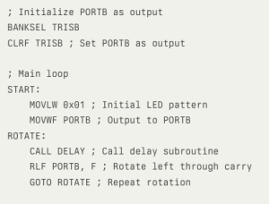
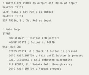
This appendix provides brief information to support the main content of the module in this course.It includes summaries and key points regarding the 8085 instruction set and the PIC16(L)F18855/75 ADC2 module, along with practical code examples and configuration details.
8085 Instruction Set Overview
The 8085 microprocessor has a rich set of instructions that can be broadly categorized into several types:
- Data Transfer Instructions:
- MOV: Copy data between registers or between a register and memory.
- MVI: Move immediate data to a register or memory.
- LDA/STA: Load or store the accumulator from/to memory.
- LDAX/STAX: Load or store the accumulator using indirect addressing.
- Arithmetic Instructions:
- ADD/ADC: Add register or memory to the accumulator, with or without carry.
- SUB/SBB: Subtract register or memory from the accumulator, with or without borrow.
- INR/DCR: Increment or decrement a register or memory.
- DAD: Add register pair to HL pair.
- Logical Instructions:
- ANA/ORA/XRA: AND, OR, or XOR register or memory with the accumulator.
- CMA: Complement the accumulator.
- CMP: Compare register or memory with the accumulator.
- Branch Instructions:
- JMP: Unconditional jump to a specified address.
- JC/JNC, JZ/JNZ: Conditional jumps based on the status flags.
- CALL/RET: Call and return from subroutine.
- RST: Restart from a specific address.
- Stack, I/O, and Machine Control Instructions:
- PUSH/POP: Push or pop data to/from the stack.
- IN/OUT: Input or output data from/to an I/O port.
- NOP: No operation.
- HLT: Halt the processor.
PIC16(L)F18855/75 ADC2 Module Configuration
The ADC2 module in the PIC16(L)F18855/75 microcontroller allows for the conversion of analog input signals to 10-bit binary representations. Key configuration steps include:
- Port Configuration:
- Set the I/O pin as an input by configuring the TRIS register.
- Configure the pin as an analog input by setting the ANSEL register.
- Channel Selection:
- Use the ADPCH register to select the desired analog input channel.
- Voltage Reference Selection:
- Configure the ADREF register to select the positive and negative voltage references.
- Conversion Clock Source:
- Select the ADC conversion clock source via the ADCLK register and the ADCS bit of the ADCON0 register.
- Interrupt Control:
- Enable ADC interrupts by setting the ADIE bit in the PIE1 register and the PEIE and GIE bits in the INTCON register.
- Result Formatting:
- Choose between left-justified and right-justified formats for the 10-bit conversion result using the ADFRM0 bit of the ADCON0 register.
- Starting and Completing a Conversion:
- Enable the ADC module by setting the ADON bit of the ADCON0 register.
- Start a conversion by setting the ADGO bit.
- Upon completion, the ADGO bit is cleared, and the conversion result is stored in the ADRESH:ADRESL registers.