Part 2: Detailed Configuration and Operation of the PIC16(L)F18855/75 ADC2 Module
Detailed Configuration of the ADC2 Module
When configuring and using the ADC2 module, several functions must be considered to ensure accurate and efficient analog-to-digital conversions. These include port configuration, channel selection, voltage reference selection, conversion clock source, interrupt control, result formatting, and more.
1.1 Port Configuration
To use the ADC2 module for converting analog signals, the I/O pins must be configured appropriately:
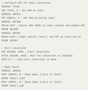
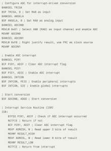
- Set the associated TRIS bit to configure the pin as an input.
- Set the associated ANSEL bit to configure the pin as an analog input.
Example:
1.2 Channel Selection
The ADC2 module supports multiple input channels, which can be selected using the ADPCH register. Available channels include:
- Eight PORTA pins (RA<7:0>)
- Eight PORTB pins (RB<7:0>)
- Eight PORTC pins (RC<7:0>)
- Eight PORTD pins (RD<7:0>, PIC16(L)F18875 only)
- Three PORTE pins (RE<2:0>, PIC16(L)F18875 only)
- Temperature Indicator
- DAC output
- Fixed Voltage Reference (FVR)
- AVSS (ground)
Example:
MOVLW 0x00 ; Select AN0 (RA0) as input channel
MOVWF ADPCH
1.3 Voltage Reference Selection
The ADPREF bits of the ADREF register control the positive voltage reference, while the ADNREF bit controls the negative voltage reference. Options include:
- Positive Voltage Reference:
- VREF+ pin
- VDD
- FVR 1.024V
- FVR 2.048V
- FVR 4.096V
- Negative Voltage Reference:
- VREF- pin
- VSS
Example:
1.4 Conversion Clock Source
The conversion clock source is selected via the ADCLK register and the ADCS bit of the ADCON0 register. Options include:
- FOSC/(2*(n+1)) (where n is from 0 to 63)
- FRC (dedicated RC oscillator)
Example:
MOVLW 0x03 ; Set ADC clock source to FOSC/8
MOVWF ADCLK
2. Starting and Completing a Conversion
2.1 Starting a Conversion
To start a conversion, the ADC module must be enabled, and the ADGO bit must be set. Conversions can be initiated by:
- Software setting the ADGO bit
- An external trigger
- Continuous-mode retrigger
Example:
BSF ADCON0, ADON ; Enable ADC module
BSF ADCON0, ADGO ; Start conversion
2.2 Completion of a Conversion
Upon completion of a conversion:
- The ADGO bit is cleared.
- The ADIF interrupt flag bit is set.
- The conversion result is stored in the ADRESH:ADRESL registers.
Example:
BTFSC ADCON0, ADGO ; Wait for conversion to complete
GOTO $-1 ; Loop until conversion is done
MOVF ADRESH, W ; Read upper 2 bits of result
MOVWF RESULT_HIGH
MOVF ADRESL, W ; Read lower 8 bits of result
MOVWF RESULT_LOW
3. Handling ADC Results
3.1 Result Formatting
The 10-bit ADC conversion result can be formatted as either left justified or right justified, controlled by the ADFRM0 bit of the ADCON0 register.
Example:
BANKSEL ADCON0
BSF ADCON0, ADFRM0 ; Set result format to right justified
3.2 Interrupt Handling
The ADC module can generate interrupts upon completion of a conversion. The ADIF bit in the PIR1 register indicates the interrupt flag, and the ADIE bit in the PIE1 register enables the interrupt.Example:
BANKSEL PIR1
BCF PIR1, ADIF ; Clear ADC interrupt flag
BANKSEL PIE1

BSF PIE1, ADIE ; Enable ADC interrupt
BANKSEL INTCON

BSF INTCON, PEIE ; Enable peripheral interrupts
BSF INTCON, GIE ; Enable global interrupts4. Practical Examples
4.1 Basic ADC Conversion
In this part, we have explored the detailed configuration and operation of the ADC2 module in the PIC16(L)F18855/75 microcontroller. By understanding how to configure ports, select channels, choose voltage references, set conversion clock sources, and handle interrupts, you can effectively utilize the ADC2 module for accurate and efficient analog-to-digital conversions.Regular practice and reference to the official Microchip documentation will help in becoming proficient in using the ADC2 module. Always consult the latest datasheet and programming manual for the most up-to-date and detailed information on the ADC2 module and its usage.
