Understanding and designing NRF24 Transceiver Circuit using Ki-CAD
Overview of NRF24 Transceiver
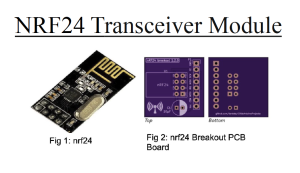
The NRF24 is a popular 2.4 GHz wireless transceiver module used in a variety of applications, including remote controls, home automation, and wireless sensor networks. It allows for wireless communication between microcontrollers and other devices over a short range, typically up to 100 meters indoors and 1,000 meters outdoors with line of sight.
Features of NRF24 Transceiver
- Frequency Range: 2.4 GHz ISM band
- Data Rate: Up to 2 Mbps
- Power Consumption: Low power consumption with power-down and standby modes
- Communication Range: Typically up to 100 meters indoors
- Interface: SPI (Serial Peripheral Interface)
- Operating Voltage: 1.9V to 3.6V
Circuit Design for NRF24 Transceiver
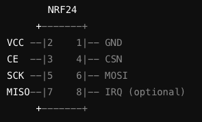
Designing a circuit with the NRF24 transceiver involves connecting it to a microcontroller (e.g., Arduino, ESP8266) and providing the necessary power and communication lines. Below is a basic schematic of how the NRF24 transceiver is connected in a circuit:
- Power Supply:
- VCC (Pin 2) -> 3.3V
- GND (Pin 1) -> Ground
- SPI Interface:
- CE (Pin 3) -> Digital I/O pin on the microcontroller (e.g., D9)
- CSN (Pin 4) -> Digital I/O pin on the microcontroller (e.g., D10)
- SCK (Pin 5) -> SCK pin on the microcontroller (e.g., D13)
- MOSI (Pin 6) -> MOSI pin on the microcontroller (e.g., D11)
- MISO (Pin 7) -> MISO pin on the microcontroller (e.g., D12)
- Additional Connections:
- IRQ (Pin 8) -> Can be connected to an interrupt pin on the microcontroller if needed.
Below is a simple schematic representation
PCB Layout for NRF24 Transceiver
Creating a PCB layout for the NRF24 transceiver involves placing the components on the board and routing the connections. The following steps outline the process using KiCad:
- Component Placement:
- Place the NRF24 module in a suitable location on the PCB.
- Place the microcontroller and any other components needed for the circuit.
- Routing:
- Route the power lines (VCC and GND) to the NRF24 module.
- Route the SPI lines (CE, CSN, SCK, MOSI, MISO) to the respective pins on the microcontroller.
- Ensure the traces are wide enough for power lines and appropriately spaced to avoid interference.
- Ground Plane:
- Create a ground plane to reduce noise and improve signal integrity.
- Design Rules Check:
- Perform a design rules check (DRC) to ensure there are no errors in the PCB layout.
Below is an example of how the PCB layout may look:
Video Lecture: Designing the NRF24 Circuit on KiCad
To complement this reading, refer to the following video lectures demonstrating the design process of the NRF24 transceiver circuit on KiCad. These videos will guide you step-by-step through creating the schematic, placing components, routing, and finalizing the PCB layout.
